Effectively Use Analog Signal Conditioning to Match Sensors to Processors
Contributed By DigiKey's North American Editors
2017-12-06
The core of most maker projects is digital, but sensors tend to be analog devices that require signal processing to interface with the processor analog inputs. However, issues of low signal amplitude, offset voltages, or interfering signals can complicate a maker’s design process by putting the signal levels outside of the digital input range of the processor’s digitizer.
Some longtime makers understand the issues, others may have forgotten the fundamentals, while for many the analog world is still shrouded in mystery. For all, this article will describe the role of analog signal processing/conditioning and provide examples of typical design requirements, constraints, and tradeoffs.
It will introduce sample devices and how to apply them, and investigate available low-cost or free design tools that can speed project design and development to help keep to a tight budget. Given that many maker projects are resource constrained, this article will also provide insight into what resources can serve multiple uses to further save on cost.
Signal processing and op amps
Analog signal processing, or conditioning, between the sensor and digital processor aims to minimize any detrimental analog effects before the signal gets into the digital domain. Furthermore it can be done cost effectively using low-cost operational amplifiers (op amps) to amplify, shift and filter sensor signals making them fully compatible with processor inputs.
Additionally, signal processing can extend the characteristics of sensors such as integrating the output of an accelerometer to obtain velocity and displacement signals.
Op amps are DC-coupled, high-gain, voltage amplifiers with differential inputs and, commonly, a single-ended output. Historically, they were used to implement analog computers for the solution of differential equations.
Due to its versatility, the op amp is now a fundamental building block for many analog circuits, including analog signal processing. They find applications in consumer, industrial, and scientific devices. They are also ideal for maker/DIY projects due to their low cost and ready availability.
Using negative feedback, the parameters of an op amp circuit, including its gain, bandwidth, and input and output impedance, just to mention a few, are governed by external components. Using good design practices, performance is mostly independent of manufacturing variations in the op amp or on environmental conditions.
Consider the Texas Instruments TL081 op amp (Figure 1).
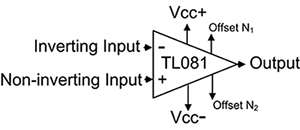
Figure 1: An outline drawing showing the connections on a Texas Instruments TL081 op amp (Image source: DigiKey)
This typical op amp has inverting and non-inverting differential input pins and a single output. The input uses a junction field effect transistor (JFET) to ensure high input impedance and extremely low bias current (30 picoamps (pA)). It has a typical large signal differential gain of greater than 100,000 at DC, and a unity gain-bandwidth product of 3 MHz. It is available in both through hole (compatible with prototyping boards) and surface-mount packages.
Matching sensors to analog-to-digital converters
Maker processors such as the Arduino boards contain analog channel inputs that are intended to read analog sensors. For example, the Arduino Uno has six analog inputs. These inputs are multiplexed into a 10-bit analog-to-digital converter (ADC). The 10-bit ADC breaks the input voltage range into 210 or 1024 voltage levels (with values from 0 to 1023).
The ADC input range is determined by the chosen analog reference voltage. In the case of the Arduino Uno the default reference voltage is 5 volts. It also has an internal reference voltage of 1.1 volts or the user can input an external reference voltage between 0 and 5 volts. The ADC will map voltages between 0 volts and the selected analog reference voltage. For the default 5 volt reference, the ADC maps 1024 levels between 0 and 5 volts, or 4.88 millivolts (mV) per level. To convert a bipolar signal, the zero level is half of the ADC range. In this example, that would be 2.5 volts. The converter codes are assigned values from 0 volts for the most negative signal value, to 5 volts for the most positive signal value, and 0 volts in the center of the range.
Now consider the signal from a transducer, such as an electret microphone, that has an amplitude of only 2 mV. The signal amplitude is less than the least significant level of the ADC in the example. To use the microphone with the ADC, the signal needs to be amplified. In addition, the signal level has to be shifted so that it is centered about 2.5 volts. These changes can be made using op amps. Moreover, the signal can be band limited to cover the desired audio range using operational amplifiers configured as a filter.
Amplifier configurations
Op amps have differential inputs and can be designed as either inverting or non-inverting amplifiers (Figure 2).
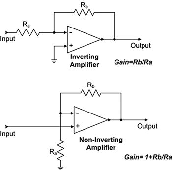
Figure 2: The two basic op amp configurations: inverting and non-inverting. (Image source: DigiKey)
The differential input of an operational amplifier has both an inverting input labeled by a minus sign (-) and a non-inverting input designated by a plus sign (+). Signals applied to the inverting input produce an output shifted by 180 degrees (inverted). In contrast, signals applied to the non-inverting input appear in-phase at the output.
The gain of each configuration is dependent only on the external resistors Ra and Rb. This is a result of the high open loop gain of the op amp and the use of negative feedback applied from the output to the inverting input via resistor Rb. Note that the gain of the inverting amplifier is determined by the ratio of Rb to Ra. The gain of the non-inverting amplifier configuration is 1 + Rb/Ra.
This shows how gain can be obtained by the op amp. The question of implementing a fixed DC offset is addressed by summing an offset voltage at one of the inputs (Figure 3).
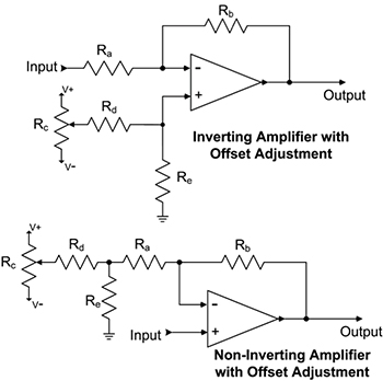
Figure 3: Techniques used to add an offset to the inverting and non-inverting op amp configurations. (Image source: DigiKey)
Offset voltages are summed into either the inverting or non-inverting inputs through a simple voltage divider. Note that the offset voltage is affected by the stage gain. This has to be kept in mind when designing the amplifier.
Design tools
There are many sources of op amp circuits that can provide amplification, filtering, or both. Op amp manufacturers offer no-cost design tools to help evaluate these circuits without actually buying the components and building prototypes. Take Texas Instruments, for example. They supply a free circuit simulation program called TINA-TI, a spice-like circuit simulator. Texas Instruments packs the program with a library of component models and circuit examples to make it easy to get started (Figure 4).
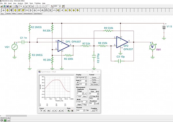
Figure 4: TINA-TI simulation of an amplifier/filter intended to match an electret microphone to an Arduino board. It provides a gain of 100 with a 300-10,000 Hz bandpass filter. (Image source: DigiKey)
This circuit uses two Texas Instruments OPA337NA-3K op amps. This op amp is designed for battery-powered devices and supports single-supply operation, JFET inputs with <10 pA bias current, and a 3 MHz gain-bandwidth product.
OP1 in Figure 4 is configured as a non-inverting amplifier with a gain of 10 (20 dB). OP2 is setup as a multi-feedback low-pass filter with a 10 kHz cutoff frequency. This stage also has a gain of 10. These two cascaded stages provide an overall gain of 100 (40 dB). The input is AC coupled, with an upper cutoff frequency of approximately 300 Hz. This, combined with the low-pass filter, yields a bandpass filter covering 300 to 10,000 Hz.
Circuit performance can be tested using built-in virtual instruments like a DVM, signal generator, oscilloscope, and signal analyzer. The circuit performance is shown on the virtual signal analyzer. The plot shows gain as a function of frequency. It verifies the gain of 40 dB over a band of 300 Hz to 10 kHz.
Biasing is also included by the voltage divider set up by R4 and R5 producing a 2.5 volt bias for the processor ADC.
The final amplifier circuit
The final amplifier circuit (Figure 5) shows the electret microphone and its bias resistor.
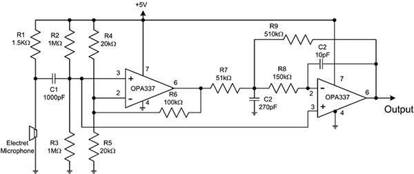
Figure 5: The completed schematic for the amplifier including the electret microphone and its associated bias resistor. (Image source: DigiKey)
This is the final version of the circuit intended to operate from the same 5 volt power source as the Arduino board. The resistor R1 provides the necessary bias current for the microphone. All of the other components are identical to the simulated amplifier in Figure 4.
Single transducer, multiple outputs
Historically, the op amp has been used to solve differential equations. This involves being able to differentiate and integrate signals. Using this capability, the output of an accelerometer can be integrated once to read velocity. If the velocity signal is integrated, then the output is displacement. This means that by using op amps to integrate signals, the output of a single transducer can produce three distinct signals. Acceleration, velocity, and displacement can all be read from a single accelerometer (Figure 6).
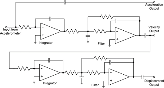
Figure 6: Use dual integrators to produce acceleration, velocity and displacement readouts from an accelerometer along with the acceleration signal. (Image source: DigiKey).
The signal from the accelerometer is output directly; it is also integrated once to produce a velocity output. The velocity signal is integrated to derive the displacement signal.
The integrator uses an op amp with a capacitor in its feedback loop. In this example, it is followed by a second op amp wired as a low-pass filter to limit the bandwidth of the signal to reduce noise. This technique is used in several commercial accelerometer signal conditioning power supplies.
When using op amps as integrators there are several things to keep in mind. The first is that integrators tend to drift; any bias current from the op amp accumulates charge on the feedback capacitor resulting in an output voltage. Using op amps with extremely low bias currents, such as the TL081 and OPA337, will minimize this problem.
When a signal is integrated there is an integration constant that is added to the signal. The value of this constant depends on the initial conditions. This circuit uses AC coupling to remove these DC constants. The result is that the velocity and displacement signal only read relative values. Therefore, in the displacement signal, you only see the change in displacement, not the absolute displacement. This is no problem for applications like vibration measurement where the change in displacement is all that is needed. It cannot be used to determine the absolute change in location of the accelerometer.
Learning more about op amps
There are several op amp training kits that are available to help investigate and learn how to apply these useful signal processing devices. One of the best is the Pro Analog system Lab kit from MikroElektronika. This kit, developed in conjunction with Texas Instruments, offers fourteen experiments using op amps and related analog processing elements. The contents of this course go well beyond the examples provided in this article.
Conclusion
Op amps are key analog signal processing components that makers and DIYers need to understand for application in projects involving sensors and digital processors. They provide gain, control offset voltages, filter analog signals, and can integrate or differentiate sensor outputs to make sure the sensor and processor interface is optimally matched. They do all this well within the limited budgets of most hobbyists.

Disclaimer: The opinions, beliefs, and viewpoints expressed by the various authors and/or forum participants on this website do not necessarily reflect the opinions, beliefs, and viewpoints of DigiKey or official policies of DigiKey.


